Ceramic Forum, Glass Manufacturing Technology and Wide-Gap Semiconductors
Analysis Services (DLTS Measurement Service)
DLTS (Deep Level Transient Spectroscopy) Method
Since the characteristics of semiconductor materials are greatly affected by very small impurities such as inherent lattice defects (crystal defects), defect evaluation is extremely important.
Since it was devised by Lang of Bell Laboratories in 1974, the DLTS method is an excellent technique to detect the electronic state (deep level) created by crystal defects with high sensitivity, and continues to be widely used.
Since it was devised by Lang of Bell Laboratories in 1974, the DLTS method is an excellent technique to detect the electronic state (deep level) created by crystal defects with high sensitivity, and continues to be widely used.By monitoring the dynamic process by which the carrier (e.g. electron) trapped in the deep level is emitted into the band (conduction band), through the transient changes in the junction capacitance of the sample, the parameters (energy levels, capture cross-section) and concentration value, spatial distribution etc. of the level can be known.
As well, the DLTS method is not only effective for measurement of discrete levels produced by single atom level defects, but also for evaluating interface states in MOS structures and continuum levels in amorphous semiconductors.Furthermore, a feature of the DLTS method is that it's superior sensitivity levels can be heightened. The impure atom detection lower limit concentration level detected by SIMS analysis, (high sensitivity surface analysis) is 10E14 atoms / cm3, however, amazingly, in the DLTS method, levels of trace concentrations of 10E9 atoms / cm3 or less can be detected depending on the conditions.
Evaluation and Analysis Services
At Ceramic Forum, we have started offering measurement and analysis services for defect evaluation in semiconductor materials / devices by the DLTS (Deep Level Transient Spectroscopy) method.
When it comes to defect evaluation methods in semiconductors, the DLTS method has merits in its detection sensitivity etc., that are not available in other analysis methods.However, considerable knowledge and experience are necessary to master the use of this method and obtain correct evaluation results.
With our equipment system sales, measurement / analysis services, and further dissemination of DLTS related technology, we would like to contribute to the development of the Japanese semiconductor industry.
Features of our Measurement / Analysis Services
- Capable of Meeting a Wide Range of Measurement Needs
Although the DLTS method is certainly a highly sensitive means of measurement, the physical properties of semiconductors are diverse.For example, in so called semi-insulating semiconductors and ultra-thin layer semiconductors with depletion layers covering the whole sample, transient changes in junction capacitance can no longer be measured and normal capacity DLTS method is ineffective.
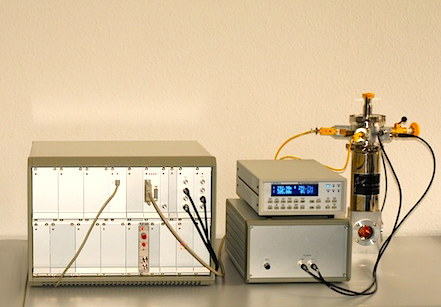
In such samples, the current mode based PITS method and TSC method are effective.The FT1030 is our standard measurement system, as it can meet a wide range of measurement needs according to the physical properties of the sample.
- Supported by Professional Engineers
The professional engineers in charge of our measurement / analysis services have been involved for many years in semiconductor R & D, as well as defect evaluation by the DLTS method.Defect levels may often exhibit complicated phenomena such as metastable behavior etc. making it difficult to interpret DLTS measurement results.With their abundant knowledge and experience, our staff can solve such problems.