Ceramic Forum, Glass Manufacturing Technology and Wide-Gap Semiconductors
GaN Epi Services
Features of GaN Epi Services
Ceramic Forum began handling GaN Epi Services from Poland's Seen Semiconductor in 2016.Seen Semiconductor provides high quality Epi services by engineers with 20 years of experience.Although centered mainly on providing GaN epitaxy, they also offer a wide variety of epitaxial structures such as AlInGaN, ALN, SiC, graphene etc.
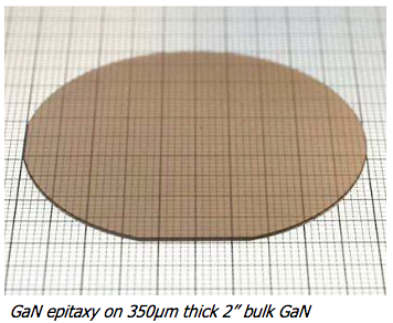
As base substrate, free-standing GaN substrate, sapphire, Si, SiC, InP, GaAs etc. can be used. The surface orientation can be c-plane, non-polar plane, semi-polar plane etc. according to customers requests.
As base substrate, free-standing GaN substrate, sapphire, Si, SiC, InP, GaAs etc. can be used. The surface orientation can be c-plane, non-polar plane, semi-polar plane etc. according to customers requests.
Manufacturer Profile
Seen Semiconductor (Poland)
A spin-off company from the Polish Academy of Sciences, Institute of High Pressure Physics (Unipress) (2011), specializing in III-V genera epitaxial growth for not only GaN, but also InP, GaAs, AlGaN, AlN etc.Featuring a high degree of flexibility to accommodate orders of simple structures to complicated structures.
Epi-types Provided
- Epi services for GaN power devices (HEMT, Diode)
- Epi services for GaN high frequency devices (HEMT)
- Graphene layer formation
- Epi Structure for LED, Laser, VCSEL, Varactors, Photodetectors
Specifications
Please see the following page for specifications.⇒ Seen Semiconductors Product Page