Ceramic Forum, Glass Manufacturing Technology and Wide-Gap Semiconductors
Phystech DLTS Measuring Device (FT1030)
The Phystech (Germany) DLTS Measuring Device (FT1030 HERA-DLTS) sold by our company, in addition to being a highly sensitive measuring system essential for DLTS measurements, is also equipped with sophisticated, high-functionality software capable of dealing with defect evaluation for various semiconductor materials.
FT 1030 DLTS measurement mode
FT 1030 DLTS measurement mode: The FT1030, in addition to the basic DLTS measurement mode, has an ICTS (Isothermal Capacitance Transient Spectroscopy) mode for time domain measurement under fixed temperatures.
The FT1230 can meet the needs for optical DLTS / ICTS using optical pulses, CC mode (Constant Capacitance-DLTS), current mode DLTS / ICTS, as well as PITS (Photo-induced current Transient Spectroscopy) method, effective for measuring semi-insulating semiconductors and ultra-thin layers where the entire sample is depleted, and TSC method (Thermally Stimulated Current) etc.
Current mode, and DLTS / ICTS measurement, are also applied to defect evaluation in three-terminal elements such as FET etc.Please see the table below for details.
FT1030 DLTS Measurement Mode
スクロールで図全体をご覧いただけます。
| Measurement Method (Mode) |
Capture Pulse / Physical Quantity Measuring |
Features and Applications |
|---|---|---|
| ①DLTS | Features and Applications | ☆ Default measurement mode in DLTS.Default measurement mode in DLTS. ・Applicable not only to discrete levels but also to the evaluation of MIS interface state and continuum levels in amorphous semiconductors. |
| ②I-DLTS/ICTS (Current-) |
Voltage / Current | ☆ Voltage / Current ・Effective for evaluation with an ultra-thin layer semiconductor sample fully depleted in the carrier emission process |
| ③CC-DLTS/ICTS (Constant Capacitance-) | Voltage / Voltage | ☆ The measurement range is kept constant due to feed back to the bias voltage so that the capacitance in the carrier emission process is constant (constant depletion layer width). ・The measurement range is kept constant due to feed back to the bias voltage so that the capacitance in the carrier emission process is constant (constant depletion layer width). ・Evaluation with an ultra-thin layer semiconductor sample fully depleted in the carrier emission process ・Able to do a precise measurement of the MIS interface state density profile |
| ④D-DLTS (Double correlation-) |
Voltage / Capacitance | ☆Information on the spatial local area is obtained from the difference measurement of the capacitance transient waveform at two different bias voltages. ・Measurement of depth profiles of defect concentration ・Evaluation of local electric field effect (Poole-Frenkel effect) on carrier emission process |
| ⑤O-DLTS (Optical-) |
Optical / Capacitance | ☆ The carrier capturing process is performed by optical pulse application. ・Able to evaluate minority carrier traps in Schottky junction samples ・Evaluation of optical parameters (photoionization cross section etc.) in defect levels |
| ⑥ICTS (Isothermal Capacitance Transient Spectroscopy) |
― | ☆ Transient capacity measurement is done in a time domain under constant temperature.Able to apply measurement similar to ① - ⑤Effective when there is a large change in physical properties due to measurement temperature etc. ・Evaluation of defects in amorphous semiconductors etc. |
| ⑦PITS (Photo-induced current Transient Spectroscopy) |
Optical / Current | ☆ Equivalent to I-DLTS measurement using optical pulses. ・Defect evaluation in semi-insulating semiconductor samples that cannot be measured for transient changes in capacitance ・Evaluation with an ultra-thin layer semiconductor sample fully depleted in the carrier emission process |
| ⑧TSC/TSCAP (Thermally Stimulated Current/Capacitance) |
Voltage, Optical / Current, Capacitance |
☆ These are measured not in transient change but in steady state mode.The carrier emission process is measured as current or junction capacitance change, where samples which captured carriers at a low temperature were heated at a constant rate. ・Application example similar to PITS.As for TSC, it is widely applicable to research on electric charge phenomena related to non-semiconductor insulating materials (ionic crystal, resin, glass) and powder. |
| ⑨FET Characterization | Voltage圧 / Capacitance, Current |
☆ A method for directly measuring defects in three-terminal elements such as FETs. ・Able to evaluate trap concentration around the gate insulating film and active layer by DLTS measurement of gate capacitance under differing SD voltage, or by I-DLTS measurement of drain currents under varying gate voltage. |
In addition to the above, FT1030 also has various measurement applications such as trap concentration profile measurement, direct measurement of capture cross-section by capture pulse method, and Zerbst analysis etc.
One of the most important performance points of the DLTS Measuring Device is sensitivity.Due to the uniquely devised hardware / software of the FT1030, it has the following high sensitivity.
・Capacitance Meter Sensitivity : 0.01 fF
・Trap Detect Sensitivity : 10-7<10-5 ・Energy Accuracy : ±3%
In addition to the above, FT1030 also has various measurement applications such as trap concentration profile measurement, direct measurement of capture cross-section by capture pulse method, and Zerbst analysis etc.
One of the most important performance points of the DLTS Measuring Device is sensitivity.Due to the uniquely devised hardware / software of the FT1030, it has the following high sensitivity.
・Capacitance Meter Sensitivity : 0.01 fF
・Trap Detect Sensitivity : 10-7<10-5・Energy Accuracy : ±3%
Another feature of FT1030 is the HERA (High Energy Resolution Analysis) - DLTS system.
The DLTS spectrum usually has a relatively broad shape.
When there are two levels with similar energy, it is not easy to separate them by conventional DLTS method.
In order to handle this, the HERA-DLTS system realized higher energy resolution, by using proximity waveform separation software based on several new mathematical algorithms (Provencher contin and discrete; www.s-provenchre.com).
These algorithms consist of Fourier transform, Laplace transform, multi-exponential fitting, deconvolution of ICTS spectrum and DLTS spectrum, etc.Examples of use are shown below.
In HERA analysis, there are two application methods, one for capacitance (or current, voltage) transient waveform, and one for DLTS / ICTS spectrum.
Figure 1 shows a simulation example of separating and extracting two exponential carrier emission processes when Laplace transform method is applied to a capacitance transient waveform corresponding to a carrier emission process from a deep level at a certain temperature.
Also, Figure 2 shows an example of separating and extracting two levels with closely adjacent thermal emission time constants when HERA analysis is applied to the ICTS spectrum.From the same measurement at six different temperatures (Figure 3), the temperature change of the thermal emission time constant at each separate level is calculated. By displaying this on an Arrhenius plot (Figure 4), each adjacent energy level, capture cross-section, and concentration can be analyzed.
Simulation Data:
E1=0.34eV, E2=0.35eV, σ1,2=1.0E-14cm2, Amplitude1,2=1.0pF
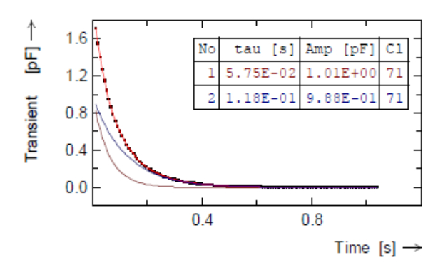
Figure 1.Separation of capacitance transient waveform by Laplace transform (○: data point, red purple solid line (1) and blue solid line (2): separated transients, red solid line: fitting result)
Figure 2.Separation of proximity peaks in ICTS spectrum (a1) by HERA analysis
(□: data point, green: peak separated by deconvolution, red: fitting result)
Figure 3.ICTS spectrum under 6 temperature conditions
Figure 4.Arrhenius Plot from the data in Figure 2 and Figure 3
An example of HERA deconvolution on DLTS spectrum is shown in Figure 5.
In this spectrum, a1 (correlation function of cosine) analysis was done. Then, the relationship between each set of thermal emission time constants and temperature, is obtained for each of the two proximity levels.
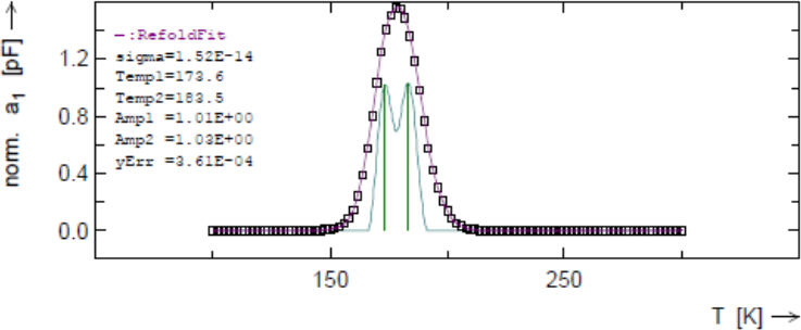
Figure 5.Separation of adjacent peaks in DLTS spectrum (a1) by HERA analysis
(□: data point, green: peak separated by deconvolution, red: fitting result)
Figure 6 shows a similar analysis performed on 23 kinds of correlation functions and an Arrhenius plot of the results obtained (Maximum analysis).
In the figure, the analysis results of parameters and concentrations for the 2 adjacent levels are shown.
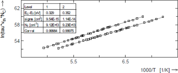
Analysis similar to that in Figure 5 was done on 23 correlation functions and an Arrhenius plot of the results was obtained (Maximum analysis).
As described above, PhysTech's HERA-DLTS: FT 1030 is a high functioning defect evaluation and analysis system, which has the highly diverse application analysis software required for defect evaluation, in addition to basic high precision and high-resolution performance using a new mathematical algorithm.